Photonics 2.0: How Light-Based Computing Will Make Silicon Obsolete
advertisement
The computing industry stands on the brink of a photonic revolution that promises to overcome the fundamental limitations of silicon-based electronics. Photonics 2.0 represents not merely an incremental improvement but a complete paradigm shift from electron-based computation to light-based processing, leveraging breakthroughs in integrated photonics, metamaterials, and quantum light manipulation. Where traditional computing struggles with heat dissipation and energy efficiency at nanoscale dimensions, photonic systems operate with minimal thermal generation while achieving data transfer rates approaching the speed of light. This transition from electrons to photons addresses the three critical constraints of Moore's Law—power consumption, heat generation, and signal delay—that have plagued semiconductor advancement for decades.
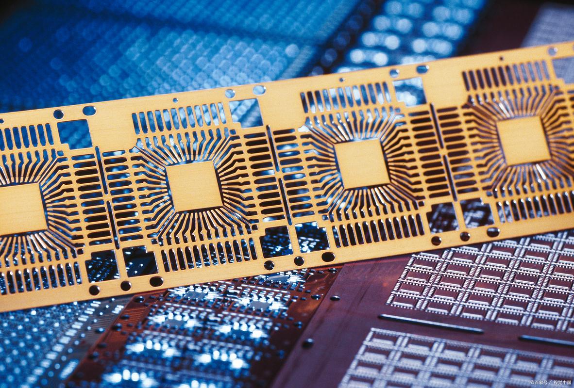
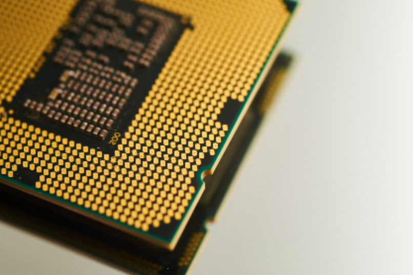
Modern photonic processors integrate thousands of optical components on single chips, manipulating light through microscopic waveguides, modulators, and detectors fabricated using semiconductor-compatible processes. Unlike first-generation optical computing that merely used light for communication between electronic components, Photonics 2.0 implements complete computational functions in the optical domain. Researchers at MIT have developed photonic neural networks that perform matrix multiplication at the speed of light, achieving computational densities 1000 times greater than electronic counterparts while consuming less power. These systems exploit light's inherent parallelism—multiple wavelengths can travel through the same waveguide simultaneously without interference, enabling massively parallel processing that electronic systems cannot match.
The most significant advances emerge in specialized computing applications where photonics offers insurmountable advantages. Quantum photonic processors can generate and manipulate entangled photon pairs for quantum computing applications, operating at room temperature unlike many competing quantum technologies. Analog optical computers excel at solving optimization problems and differential equations directly in the optical domain, bypassing the digital abstraction layer that limits electronic computers. Perhaps most impressively, photonic AI accelerators are demonstrating unprecedented efficiency in neural network inference tasks, processing complex deep learning models with energy consumption reduced by orders of magnitude compared to GPU clusters.
Material science innovations are driving photonic computing toward practical implementation. Programmable photonic circuits using phase-change materials can dynamically reconfigure optical pathways, creating field-programmable photonic arrays that adapt to different computational tasks. Non-linear optical materials with enhanced Kerr effects enable all-optical switching without conversion to electronic signals, maintaining the speed advantage throughout the computation process. Heterogeneous integration techniques now allow III-V semiconductor optical components to be integrated alongside silicon photonic elements, combining the best properties of different material systems on single chips.
The transition to photonic computing follows a different scaling paradigm than Moore's Law. Rather than simply shrinking components, photonic scaling increases computational density by adding wavelength channels through wavelength-division multiplexing and enhancing modulation speeds. This approach has enabled bandwidth densities exceeding 10 terabits per second per millimeter of chip edge, far beyond what electrical interconnects can achieve. Energy efficiency continues improving exponentially as well, with recent photonic chips demonstrating attojoule-per-bit operations—nearly 1000 times more efficient than advanced electronic processors.
Implementation challenges remain substantial but surmountable. Coupling losses between optical components have been reduced through inverse-designed nanophotonic structures that maximize energy transfer. Thermal stability issues are addressed through athermal waveguide designs that maintain optical properties across temperature variations. Perhaps most importantly, fabrication processes have achieved CMOS compatibility, allowing photonic circuits to be manufactured in existing semiconductor foundries with minimal process modifications. This manufacturing compatibility significantly lowers the barrier to commercial adoption compared to technologies requiring completely new fabrication facilities.
The implications extend beyond raw computing power to entire system architectures. Photonic memory systems using nanophotonic switches promise access times measured in picoseconds rather than nanoseconds. Optical interconnects enable new distributed computing architectures where physical distance becomes less relevant to system performance. Even consumer devices will benefit—imagine smartphones that perform complex AI tasks locally without draining batteries or data centers that reduce their energy consumption by 90% while increasing computational capacity.
As photonic computing matures, it's creating a new ecosystem of applications that were previously impractical. Real-time brain-computer interfaces could process neural signals with minimal latency and power consumption. Autonomous vehicles might make decisions based on photonic processing of sensor data without computational delays. Scientific research could simulate complex systems in hours rather than years. This technological transition represents more than just faster computing—it enables fundamentally new capabilities that will reshape technology, business, and society in ways we are only beginning to imagine.
(Writer:Tick)
Related Articles